AMD has inaugurated a new research and development (R&D) center in Bengaluru, India, and it is called AMD Technostar R&D Campus. According to the chipmaker, it is the company’s largest design center globally, spanning across 500,000 square feet and employing around 3,000 engineers. According to AMD, the Technostar Campus is a part of the company’s plan that involves investing $400 million in India, which it announced at the Semicon India 2023 event.
At the Technostar R&D Campus, AMD plans to focus on the “design and development of semiconductor technology including 3D stacking, artificial intelligence, machine learning, and more.” In the press release, the company says that this campus will serve as a “centre of excellence for the development of leadership products across high-performance CPUs for the data center and PCs, data center and gaming GPUs, and adaptive SoCs and FPGAs for embedded devices.”
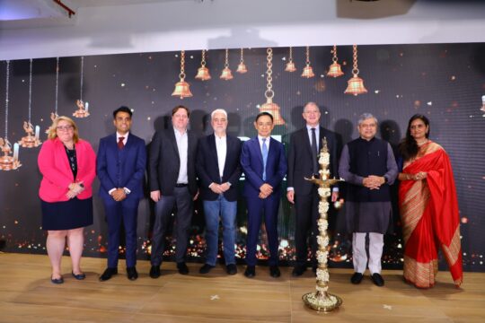
The R&D center was inaugurated by Ashwini Vaishnaw, Union Cabinet Minister for Railways, Telecommunications, Electronics and Information Technology, Government of India. Many high-level officials from AMD were also present at the inauguration event, including Mark Papermaster, Chief Technology Officer (CTO), and David Wang, Senior Vice President (SVP) of Radeon Technologies Group. The site will be led by Deepak Agarwal.
The campus has “modern R&D labs spread over 60,000 square feet and a large demo centre for visitors to experience AMD products and solutions.” The company says “office space celebrates Indian art and craft, with huddle spaces and conference rooms designed to foster collaboration and creativity.” It also has a cafeteria that is “acoustically engineered to host gatherings of more than 2000 employees and a gym and a yoga centre to promote the holistic health and well-being of AMD employees.”