One of the most important tools used by foundries in the manufacture of cutting-edge chips is the extreme ultraviolet lithography (EUV) machine. With billions of transistors inside these small components (there are 19 billion transistors inside each A17 Pro SoC used on the iPhone 15 Pro and iPhone 15 Pro Max), the circuitry patterns etched on the silicon wafer that eventually gets sliced into individual dies have to be ridiculously thin. And that is where the EUV machine comes in.
Dutch firm ASML is the only company that makes EUV machines. About the same size as a school bus, each machine costs $150 million. ASML was expected to ship 60 EUV machines this year. And today, per Tom’s Hardware, the company shipped the first second-generation EUV machine known as the High-NA EUV machine. The first shipment is headed to Intel which will use it for its 18A (18 angstroms) 1.8nm process node due to start mass production in 2025.
In 2025, when both TSMC and Samsung Foundry are expected to commence with 2nm mass production, Intel’s 1.8nm node will give it process leadership in the industry. Intel is believed to be shelling out $300 million-$400 million for the High-NA EUV machine. An ASML spokesman said today, “We are shipping the first High NA system and announced this in a social media post today. It goes to Intel as planned and announced earlier.”
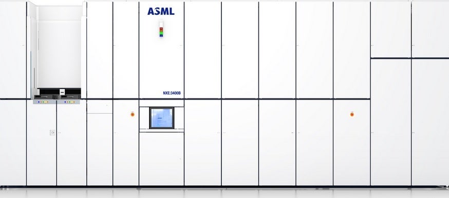

ASML expected to ship 60 EUV machines this year
As we told you two years ago, High-NA stands for high numerical aperture. The higher the NA number, the higher the resolution of the pattern being etched onto the silicon wafer. While current EUV machines have an aperture of .33 (equivalent to a resolution of 13nm), the High NA machines have an aperture of .55 (equivalent to a resolution of 8nm). With a higher resolution pattern transferred to a wafer, the foundry could avoid having to run a wafer through the EUV machine twice to add additional features saving both time and money.
The High-NA EUV machine is all about reducing the size of transistors and increasing density to pack more transistors inside a chip. The higher a chip’s transistor count, the more powerful and energy-efficient it is. With the High-NA machine, features can be made 1.7x smaller with a 2.9x increase in density.
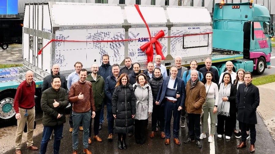

ASML employees stand in front of a container containing the unassembled High-NA EUV machine heading to Intel
Shipping the High-NA EUV machine is no easy task. It is broken down into 13 big containers and 250 crates. Assembling the machine might be a little harder than putting together the bicycle you bought your kid for the holidays.


