The world’s two top foundries are, in order, TSMC and Samsung Foundry. Both started working extreme ultraviolet (EUV) lithography into their chip production back in 2019 which set the stage for chips to be made using nodes under 7nm. You see, lithography machines etch circuitry patterns onto silicon wafers to help build semiconductors. The lower the process node, the smaller the chip’s feature set including transistors.
Smaller transistors mean that more of them can fit inside a die; with tens of billions of transistors inside modern chipsets (for example, the 3nm A17 Pro sports 20 billion transistors in each chip!) these circuitry patterns must be extremely thin. And that is where the EUV lithography machine comes into play. It is built by just one company in the entire world, Dutch firm ASML. Keep in mind that the higher a chip’s transistor count, the more powerful and/or energy-efficient that chip is.


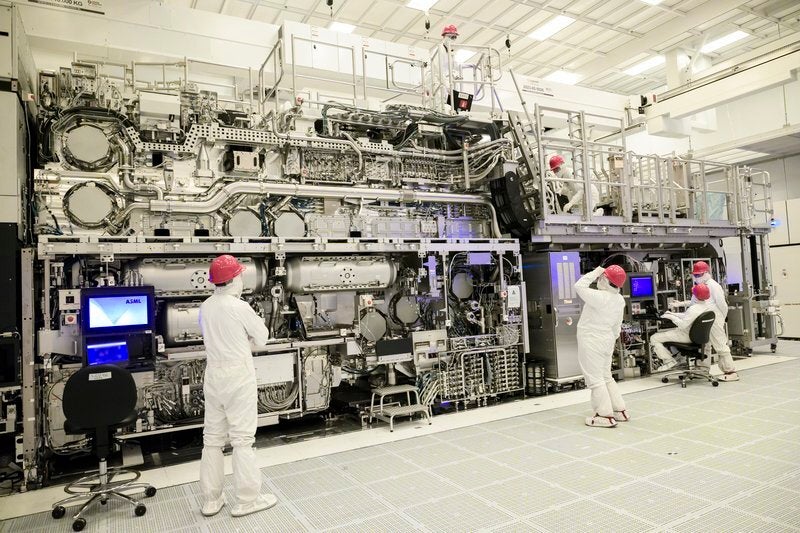
A high-NA EUV lithography machine being assembled in Oregon. | Image credit-Intel
While the first-gen EUV helped foundries crack the 7nm node, the high-NA EUV machines will take chip-making to the 1nm process node and lower. ASML says that the numerical aperture, which is what the “NA” abbreviation stands for in high-NA, measures the ability of the optical system to collect and focus light. The higher NA of .55 on the next-gen machines is what helps the new gear perform better than the first-gen machines.
“Intel expects to use both 0.33NA EUV and 0.55NA EUV alongside other lithography processes in developing and manufacturing advanced chips, starting with product proof points on Intel 18A in 2025 [1.8nm] and continuing into production of Intel 14A [1.4nm]. Intel’s approach will optimize advanced process technology for cost and performance.
However, Intel is still dealing with low yields, red ink, and a tumbling stock price which got the company’s shares booted from the U.S. stock market’s 30-stock Dow Industrial bellwether where it was replaced by Nvidia. Things are going so poorly for Intel that it is outsourcing its production down to 3nm to TSMC.


